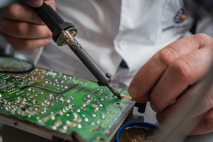






PCBA Service
SMT/THT Capability----
Detailed process envelope: package range, precision placement, soldering processes and the complete test system behind every order.
Get Quote±25μmPlacement Accuracy
0.25mmMin. BGA Pitch
Process Parameters at a Glance
| Smallest Package | 01005 / 0201 |
| Min. BGA Pitch | 0.25 mm |
| Placement Accuracy | +/-25 um |
| Max. Panel Size | 460 x 360 mm |
| THT Processes | Wave / selective / manual |
| Inspection | SPI + AOI + X-ray |
Inspection & Test System
Standard inspection gates on every order, expandable to your test plan.
SPI Paste Inspection
3D SPI verifies paste thickness and alignment, catching issues before placement.
100% AOI
Post-reflow full inspection for offset, tombstones, polarity and bridges.
X-ray Sampling
BGA and QFN joints verified by X-ray sampling - hidden joints fully covered.
ICT · FCT
In-circuit and functional testing available, executed per your test plan.
Service Process
1
Engineer Review
Complex boards reviewed by engineers before production
2
Solder Paste & SPI
Laser stencil with 3D solder paste inspection
3
Placement & Reflow
High-speed placement with nitrogen reflow
4
THT & Soldering
Wave / selective soldering for through-hole
5
AOI & Testing
100% AOI, ICT/FCT on request
Frequently Asked Questions
SPI on paste, 100% AOI after reflow, and X-ray sampling on BGA/QFN joints. ICT/FCT can be added per your test plan.
Yes, mixed assembly is our standard flow: reflow first, then wave/selective soldering or hand soldering.
All standard processes are RoHS lead-free; leaded processes are available for specific legacy requirements.